Voltage Regulation
Voltage Regulation is an important part in power design for electronic circuits as regulators are able to stabilize the voltage the circuits receive. This is especially important in high precision circuits where a stable power source is necessary for the circuit to operate properly. Voltage Regulators maintain a steady DC voltage within the regulator’s operating range.Building a Voltage Regulator
Figure 1 shows the Voltage Regulator Circuit that is constructed in Lab 4. The key elements of the circuit are resistors, Bipolar Junction Transistors (BJT), a Zener Diode, and an Op-Amp. These components are connected in a specific topology to create the Voltage Regulator.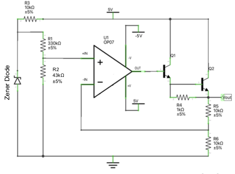
Figure 1: Voltage Regulator Circuit
Dr. Joseph Young
Reference Voltage
The Zener Diode is used to create a reference voltage. As noted in Horowitz and Hill’s The Art of Electronics1, “When [a zener diode is] connected in parallel with a variable voltage source so that it is reverse biased, a Zener diode conducts when the voltage reaches the diode's reverse breakdown voltage. From that point on, the low impedance of the diode keeps the voltage across the diode at that value.” The Zener Diode in Figure 1 is in parallel with the rest of the circuit, meaning that the diode is providing a reference for the Op-Amp and BJTs to use. According to the 1N5226 Zener Diode Datasheet2, the zener diode that is used in this circuit has a nominal Zener (Breakdown) Voltage of 3.3V at 20 mA. While this value differs from what is found in practice, it dictates the reference voltage for the rest of the circuit. It is important to note that Zener Diodes often require a bias current. In the circuit diagram shown in Figure 1, the R3, 10 kΩ resistor is required to put the Zener Diode in breakdown mode.Error Amplifier
The Op-Amp topology shown in Figure 1 is an Error Amplifier. An error amplifier (as the name suggests) amplifies the error (difference) between the non-inverting and inverting input. The op-amp itself wants to keep the voltage between the two inputs. The non-inverting input of the op-amp is the reference voltage of the zener diode divided down by R1 and R2. The inverting input is the feedback from the op-amps output. This means that the output voltage of the op-amp is regulated by the reference voltage and resistor network. Quantitatively, the output voltage is expressed in terms of the Non-Inverting Op-Amp equation.
Vout = Vin(1+
Rf
R
)
Vout = (VZener)(R1 and R2 Network)(1+
Rf
R
)
Transistors
The transistors on the right side of Figure 1 form a Darlington Pair, which is used to amplify the output of the op-amp in this circuit. A NPN Darlington Pair is created when the emitter of the first transistor is connected to the base of the second transistor. As BJTs are current driven devices, the Darlington Pair will amplify the input current. Each transistor in the pair will have some amplification coefficient given how the transistor is used in the circuit. This coefficient, hFE (β is also commonly used), is used to describe how much the transistor amplifies the current from the input to the output. When the BJT is has a more positive collector than emitter, has base-emitter and base-collector junctions that behave like diodes, and falls within standard operating range,3 the individual transistor’s collector current can be modeled as:IC=IB*hFE
IC≈IB1*hFE(1)+IB2*hFE(2)
IC≈IB1*hFE(1)+(IB1*hFE(1)*hFE(2))
IC≈IB1*hFE(1)(1+hFE(2))
The coefficient h_FE for the Darlington Pair can also be expressed as the product of the two amplification coefficients when hFE(1)>> 1:
hFE≈hFE(1)*hFE(2)
Lab 4 Solutions.docx
References
1) Horowitz, Paul; Hill, Winfield (1989). The Art of Electronics(2nd ed.). Cambridge University Press. pp. 68–69. ISBN 0-521-37095-7.2) https://www.futurlec.com/Diodes/1N5226.shtml
3) Horowitz, Paul; Hill, Winfield (2015). The Art of Electronics(3rd ed.). Cambridge University Press. p. 72. ISBN 978-0-521-80926-9.