MOSFETs
Metal Oxide Semiconductor Field Effect Transistors (MOSFETs) are used extensively in digital circuits and logic. MOSFETs have 3 terminals: Source, Gate, and Drain. MOSFETs conduct current across the Source and Drain when the Gate reaches a Threshold Voltage, V_Th.N-Type and P-Type
Silicon lattices can be doped to change the amount of electrons in the lattice. Silicon lattices can have some Silicon atoms replaced with Arsenic atoms to create a net negative charge on the lattice. This is because Arsenic has an extra electron than silicon in their valence shells. Conversely, Silicon lattices can have some Silicon atoms replaced with elements like Boron to create a net positive charge on the lattice. This is because Boron has one less valence electron compared to Silicon. This respectively results in N-Type and P-Type Doped Silicon lattices.NMOS, PMOS, and CMOS
MOSFETs are broken into two distinct categories: NMOS and PMOS Transistors. As shown in Figure 1, NMOS Transistors have two N-Type regions where the Source and Drain are connected. The N-Type Source and Drain are surrounded by a P-Type Substrate (also called Body or Bulk). PMOS Transistors are the complement of NMOS Transistors. As shown in Figure 1, PMOS Transistors have two P-Type regions where the Source and Drain are connected. The PMOS transistor has an N-Type substrate.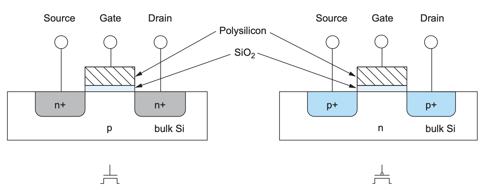
Figure 1: NMOS (Left) and PMOS (Right) Construction
Weste, Neil H. E., and David Money Harris. CMOS VLSI Design: A Circuits and Systems Perspective
CMOS configurations utilize both NMOS and PMOS transistors. They have a PMOS “Pull-Up Network” and an NMOS “Pull-Down Network”. In digital applications, Pull-Up Networks are connected to V_dd (Power) and Pull-Down Networks are connected to GND (Ground).
The NMOS Inverter
An inverter circuit outputs the complement of the input. In logical terms, if the input to the inverter is a 1, the output will be a 0. The NMOS Inverter, as shown in Figure 2, utilizes an NMOS Transistor as part of its Pull-Down Network. This Pull-Down configuration allows the inverter to drive signals to a logical 0 when the Threshold Voltage is met, which occurs when the input is a logical 1.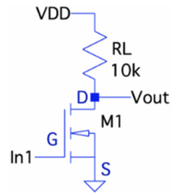
Figure 2: NMOS Inverter Circuit
Joseph Young
An NMOS Pull-Down Network is adept at driving signals to a logical 0; however, it passes a “Weak 1” when the input is 0. This is because the NMOS transistor is not efficient at passing logical 1s as the Gate to Source Voltage, V_GS, decreases as the output increases. This causes the NMOS transistor to shut off before reaching V_dd. Conversely, a PMOS Pull-Up Network is adept at driving signals to a logical 1, but passes a “Weak 0” when the input is 1.
ELEC244_lab5_solution.pdf