MOSFETs
Metal Oxide Semiconductor Field Effect Transistors (MOSFETs) are used extensively in digital circuits and logic. MOSFETs have 3 terminals: Source, Gate, and Drain. MOSFETs conduct current across the Source and Drain when the Gate-Source Voltage, V_GS, reaches a Threshold Voltage, V_Th.N-Type and P-Type
Silicon lattices can be doped to change the amount of electrons in the lattice. Silicon lattices can have some Silicon atoms replaced with Arsenic atoms to create a net negative charge on the lattice. This is because Arsenic has an extra electron than silicon in their valence shells. Conversely, Silicon lattices can have some Silicon atoms replaced with elements like Boron to create a net positive charge on the lattice. This is because Boron has one less valence electron compared to Silicon. This respectively results in N-Type and P-Type Doped Silicon lattices.NMOS, PMOS, and CMOS
MOSFETs are broken into two distinct categories: NMOS and PMOS Transistors. As shown in Figure 1, NMOS Transistors have two separate N-Type regions where the Source and Drain terminals are. The N-Type Source and Drain are surrounded by a P-Type Substrate (also called Body or Bulk). PMOS Transistors are the complement of NMOS Transistors. As shown in Figure 1, PMOS Transistors have two separate P-Type regions where the Source and Drain terminals are. The PMOS transistor has an N-Type substrate.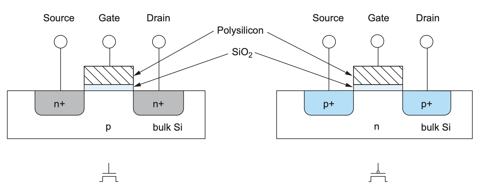
Figure 1: NMOS (Left) and PMOS (Right) Construction
Weste, Neil H. E., and David Money Harris. CMOS VLSI Design: A Circuits and Systems Perspective
CMOS configurations utilize both NMOS and PMOS transistors. They have a PMOS “Pull-Up Network” and an NMOS “Pull-Down Network”. In digital applications, Pull-Up Networks are connected to V_dd (Power) and Pull-Down Networks are connected to GND (Ground).
The NMOS Inverter
An inverter circuit outputs the complement of the input. In logical terms, if the input to the inverter is a 1, the output will be a 0. The NMOS Inverter, as shown in Figure 2, utilizes an NMOS Transistor as part of its Pull-Down Network. This Pull-Down configuration allows the inverter to drive signals to a logical 0 when the Threshold Voltage is met, which occurs when the input is a logical 1.Note: This page utilizes "logical 0" and "logical 1" (or simply "0" and "1") to describe the logical gate input of a MOSFET. "Logical 0" as described in this page refers to the condition that the magnitude of V_GS is less than the magnitude of V_Th. "Logical 1" as described in this page refers to the condition that the magnitude of V_GS is greater than the magnitude of V_Th.
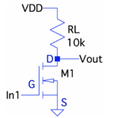
Figure 2: NMOS Inverter Circuit
Joseph Young
NMOS NOR and NAND Gates
NOR and NAND Gates are the easiest gates to construct from transistors after an inverter. Two Input NMOS NOR and NAND Gates can be constructed utilizing two NMOS Transistors. A NOR Gate outputs a logical 1 when its inputs, A and B, are A=0 and B=0. In essence, both inputs must be 0 for the output to be 1. Otherwise, the output is 0. A NAND gate outputs a logical 1 when any of its inputs are 0. This means that a NAND gate only outputs a zero for when A=1 and B=1.This logic can be used to construct an NMOS NOR Gate and NAND Gate. An NMOS NOR Gate must provide a path from V_dd to GND to output a logical 0. This can be accomplished by putting two NMOS Transistors in parallel in the Pull-Down Network as when either of them receive an input 1, a path to ground opens. An NMOS NAND Gate can be constructed using similar logic. Since a path to ground must open when both inputs are 1, the Pull-Down Network must consist of two NMOS transistors in series.
CMOS Logic
As mentioned above, CMOS circuits utilize both NMOS Pull-Down Networks and PMOS Pull-Up Networks to create logic. CMOS design is more prevalent than pure NMOS and PMOS designs as CMOS topologies mitigate many of the drawbacks of using only one type of technology. NMOS designs waste a lot of power when idling and are very susceptible to noise. PMOS designs also waste a lot of power, and they are slower compared to NMOS and CMOS circuits. This is because the PMOS transistor utilizes holes as its primary charge carrier, which have a lower mobility compared to electrons.The CMOS Inverter
A CMOS Inverter can be created by considering how PMOS and NMOS Inverters operate. The PMOS inverter operates similarly to the NMOS inverter described above; however, the PMOS inverter utilizes complementary logic. The PMOS inverter utilizes a single PMOS transistor in a Pull-Up Configuration. When the input to the gate of the PMOS transistor is a logical 0, current flows through the transistor, which results in a logical 1. When the PMOS transistor has an input of a logical 1, the transistor enters cutoff mode and prevents the flow of current through the transistor. This results in a logical 0.The CMOS inverter is composed of a single PMOS transistor in a Pull-Up network and a single NMOS transistor in a Pull-Down network. The drain of the PMOS transistor is connected to the drain of the NMOS transistor. The gate terminals of both transistors are connected to the same input signal. The output of the CMOS inverter is the connection between the two transistors. The CMOS inverter outputs a logical 1 when the input is a logical 0, as the PMOS transistor allows for the flow of current from V_dd while the NMOS transistor blocks the flow to GND. Conversely, the CMOS inverter outputs a logical 0 when the input is a logical 1 as the PMOS transistor prevents the flow of current from V_dd.
ELEC244_lab5_solution.pdf