Impedance Matching Test Board
My personal goal for this project was to learn how to use Altium EDA to design a Printed Circuit Board (PCB) whose traces are Impedance matched. This project was originally created as part of a class project, but I extended the scope of the project by designing the board using Altium’s Impedance Profile Tool. The purpose of the project was to route two differential pair wires on a 6 Layer PCB. The two differential pair wires would go between two different signal layers. Another goal of the project was to test the PCB differential wires using HyperLynx SI/PI.The following were the major constraints of the project:
- Must follow the OSHPark 6 Layer PCB Manufacturing Guidelines
- Differential Traces must be Impedance Matched to 100 Ω (50 Ω Single Ended)
- The differential pair wires must have 4 Vias per individual wire
- The total wire length for each differential pair wire must be 6 inches
- Maximum undershoot and overshoot of 140 mV
Pictured below in Figure 1 is the PCB. The two differential pairs were intentionally designed to be perpendicular to prevent any electromagnetic interference between the two pairs.
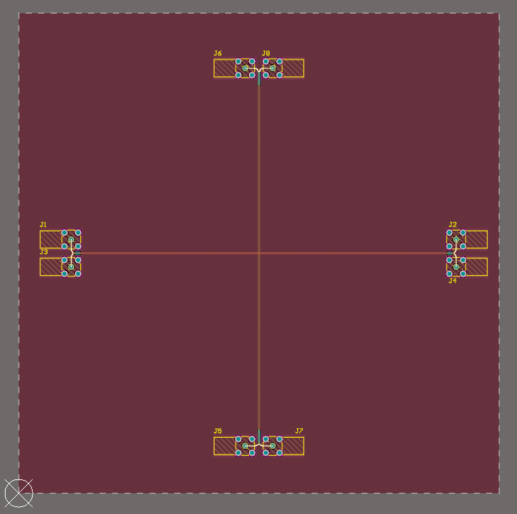
Figure 1: PCB Layout
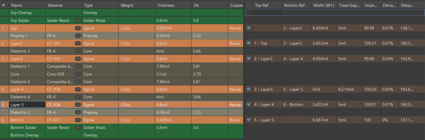
Figure 2: Altium Impedance Profile
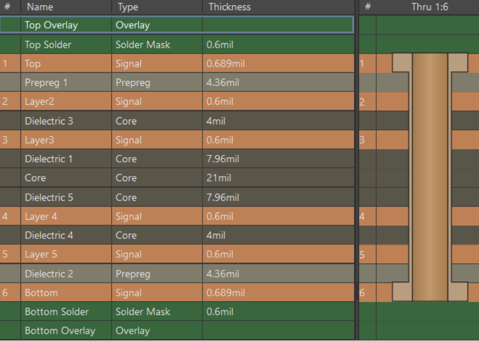
Figure 3: Altium Via Profile
- Perpendicular signal wires across layers to minimize crosstalk
- Curved signal turns instead of 90 degree signal turns
- Use of ground planes to mitigate EMI.
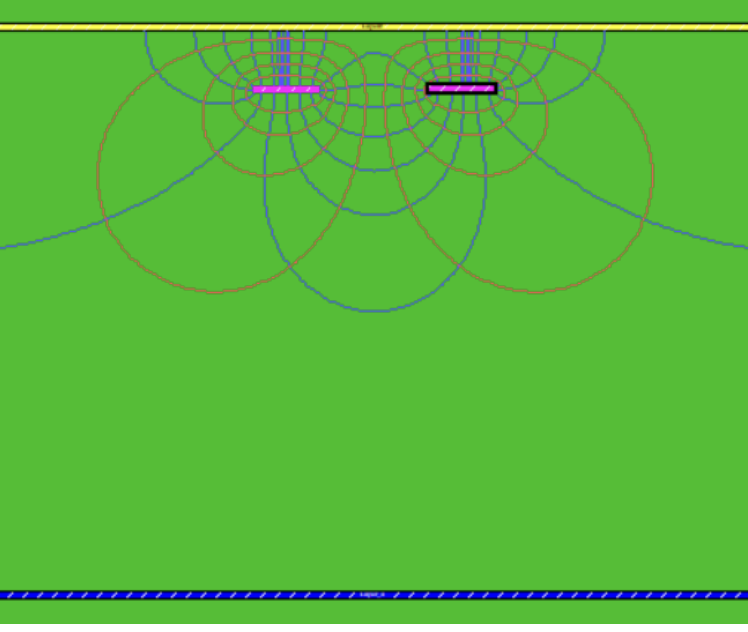
Figure 4: Layer 3 Electromagnetic Field
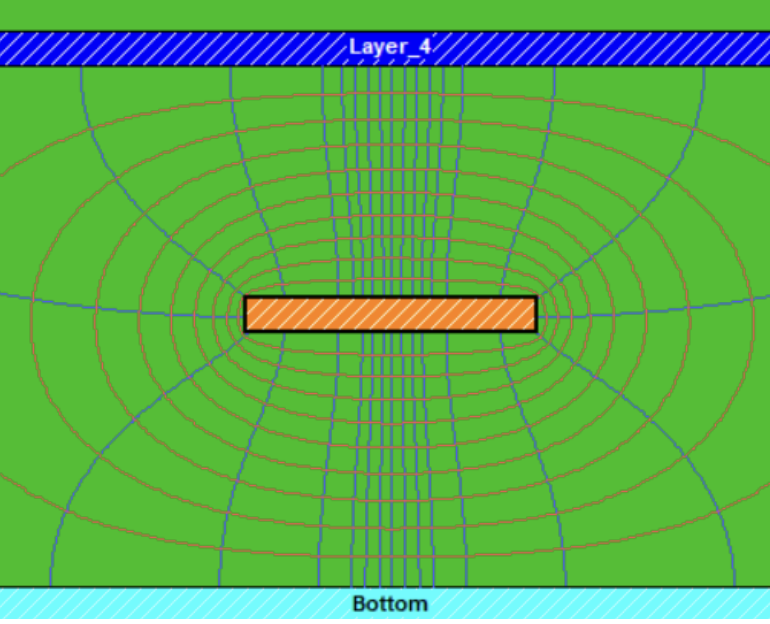
Figure 5: Layer 5 Electromagnetic Field
The following slides were used as the submission for the class project. The slides detail the design choices from the PCB and explain the HyperLynx simulation results.